|
Just Another Board Design, But With Integrity
By Werner Rissiek, Board Integrity Solutions Manager of Zuken
The ever increasing number of constraints inflicted on PCB design engineers provides a constant challenge and ensures their skills remain in high demand. Tools for checking EMI and signal integrity, that can be integrated into the design flow, are helping to ease the pressure.
The near apoplexy created by the necessary introduction of the EMC Directive in the 1990s has subsided, as some predicted at the time, to just another constraint for the hard working design engineer. Ensuring that your product has sufficient immunity to electromagnetic interference (EMI), and that it does not itself interfere with other equipment, is, after all, simply good design practice. This is no different to giving due consideration to other signal integrity issues such as crosstalk, impedance and transmission line effects.
What has changed, however, is that increasing system complexity and performance has exacerbated the likelihood of signal integrity problems. Simultaneously, time to market pressures have reduced the time available to verify and modify the designs. General ‘engineering rules of thumb’ applied at the design and layout stages have, in the past, kept most designers out of trouble. However, techniques such as using lower frequency components, avoiding those with fast edge rates where possible, may be neither appropriate nor sufficient today. Lengthy design iterations are no longer an option for many companies, and as board complexity increases, it becomes an even less viable alternative.
The key to meeting the combined design constraints of quality (which includes signal integrity), cost and deadline is to start checking at the earliest possible stage of the design, and again at various stages through the process. This is achieved by integrating the right suite of tools into a constraints (or rules-based) design flow. To ensure an uninterrupted design flow, with no lengthy delays, the signal integrity tools have to be fully consistent and compatible with the board design tools and they have to produce results quickly. Further, they must operate interactively and concurrently with the design entry and physical design tools.
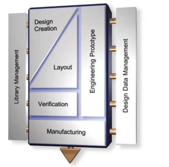
Zuken’s Hot-Stage is a powerful signal integrity and EMI prototyping tool that gives design engineers creative freedom to experiment and investigate signal performance using a virtual physical prototype. It can be closely integrated with leading schematic entry environments, including Zuken’s System Designer. (Fig.1)
Fig1: Zuken’s design flow with Engineering Prototyping as an integral element
It allows designers to carry out simulation before physical parts and connections are defined, using it effectively as a virtual scratchpad to identify viable design strategies, define topologies, and constrain the design for high speed performance.
As a high speed prototyping and signal analysis product, at the design capture stage of product design, the engineer can address such parameters as signal integrity with respect to clock frequency, drivers and receivers and transmission line impedance. He can assign design parameters, such as net topology, interconnect delay, overshoot or crosstalk limits and characteristic impedance, to selected nets or signals.
Importantly, the tools allow the designer to determine the optimum parameters for the product early in the process. Using his own judgement, the engineer can make realistic trade-offs to ensure that the end design is routeable, manufacturable and cost effective, while meeting quality standards. Significantly, while the tools make the engineer’s job easier, they do not replace his skills or knowledge. A successful PCB design will still be highly dependent on the experience of the design team.
The final set of constraints adopted are then maintained, by the tool, for use with the design as it moves through to the layout and physical design tool suite, such as Zuken’s Board Integrity Solution. The same Hot-Stage analysis environment can be used throughout the process (pre- and post- layout) to ensure that the design constraints have been obeyed. By bringing the Hot-Stage analytical tools into physical layout, the physical and logical domains are linked to ensure simultaneous compliance with electrical and physical rules.
Hot-Stage features a simulation environment to provide extensive ‘what if’ capabilities. The tool allows an engineer to experiment with the design, changing potential components and layout and assessing the impact on performance quickly. Previously this could only be achieved through hardware prototypes, which are not only time consuming to create, but can be difficult to analyse if more than one parameter has been changed, or through stand alone simulation tools, which again can be time consuming and error sensitive.
The simulation results from Hot-Stage provide the designer with a general indication of how his design is performing. The Hot-Stage simulator uses a new screening methodology to assess radiation levels by sophisticated algorithms to analyse differential mode and common mode noise. Developed by University of Missouri at Rola (UMR) and several design tool firms, including Zuken, the simulator quickly provides a yes/borderline/no result, giving the engineer the information he needs either to proceed with confidence, or backtrack if necessary to locate the root of the problem.
For signal integrity analysis, a combination of speed and performance is provided with the options of both frequency and time domain analyses. The first is fast, while the latter is more accurate, but slower. However, using the built-in calculators for delay, overshoot and crosstalk, coupled with waveform displays for rise/fall times and under- or over-shoot, the design can be fully verified before it is committed to layout.
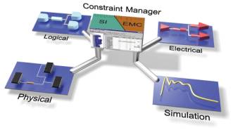
An essential feature of the design process is design management. With Zuken’s suite of design entry, layout and verification tools, this takes the form of a constraints engine presented as a spreadsheet linked to a database (Fig.2). In addition to providing a clear overview of the design at any point in the flow, the spreadsheet provides a record of the constraints set for the design, therefore ensuring consistency throughout the project. This includes the data required for layout functions such as floor planning and routing. It supports the popular approach taken by many board design teams today, whereby the design engineer will undertake to pre-route and analyse the critical nets, making adjustments as necessary, before the rest of the PCB is routed. Constraints can then be modified and refined by the designer, and are available for use in the next stage (physical design) of the project.
Fig2: Zuken’s constraint manager bridges the gap between schematic, layout, and electrical views
The importance of integrating EMI and signal integrity tools within the board design flow cannot be emphasised enough. Reducing design iterations is key to meeting time to market demands, and checking out the design up front in the process is key to reducing design iterations. The integrated design environment, using consistent data and one set of constraints, facilitates the ability to move freely between design entry, verification, pre-layout and physical design. It also provides the best support for concurrent design within larger teams and between design and layout teams.
Design engineers can feel a lot more confident about regarding EMI and signal integrity as just another set of design constraints if they have the tools to ensure these effects are fully taken into account, as just another part of the design process.
Werner Rissiek, who is now the Business Unit Manager High-Speed Routing Products, can be contacted on +49 5251 150 600.
|