Signal Integrity and EMC
By Eur Ing Keith Armstrong, Cherry Clough Consultants
|
Signal integrity is something that most electronic designers increasingly realise they need to control, as clock speeds increase, whereas EMC is something they often see as a mere regulatory burden. This article will show that signal integrity is a subset of EMC.
Understanding this concept helps to understand why it is that taking proper account of EMC from the start of a project helps improve time-to-market by reducing the number of iterations of hardware and software (when compared with the usual design practices). This would be true even if EMC compliance was not required.
Since EMC compliance is required for almost all markets worthy of the name, taking EMC fully into account at the signal integrity level makes compliance with EMC standards and regulatory requirements much quicker and easier. Continuing compliance in serial manufacture becomes much more reliable - which can reduce the frequency (and hence the on-going costs) of sample testing - and unit manufacturing costs are optimised.
For digital designers signal integrity is usually a question of maintaining noise margins, and to do this they take account of design issues such as ground bounce, crosstalk, and the creation and termination of transmission lines to minimise reflections. For analogue designers the question is one of maintaining the desired signal-to-noise ratios. Although the language used by the different camps is often incompatible, the underlying physical reality and the design techniques required (especially for PCB layout) are identical, since digital signals are just limited cases of analogue signals, as anyone who has tried to use clocks in excess of 100 MHz will have discovered.
The underlying physical reality of signal propagation can only be properly described by quantum electrodynamics, but for our purposes we can simplify this by regarding an electrical signal as being an electromagnetic wave that is guided by conductors such as metallisation patterns, lead frames, PCB tracks, connectors, wires, and cables. We need such a simplified "reality" because although we can picture propagating electromagnetic waves in our imagination, and even calculate and sketch them, and so feel that we understand how they work, no-one can reasonably claim to understand why it is that quantum electrodynamics works the way that it does.
At a lower level of simplification than wave propagation, there is always a current associated with a signal, and that current always flows in a closed loop (remember Kirchoff's law?). We discover that the current's return path is as important for the guiding of the wave that is our signal as is the send path. The physical arrangement of the send and return current paths, along with the complex impedances of the source and load and any other components attached to the signal, governs how well the electromagnetic wave is guided by the conductors (i.e. the signal's wave-guide) and how much of its energy leaks out.
Most electronic engineers, when using the word "wave-guide" think of the brass tubes used by microwave engineers. Some may realise that transmission lines are also wave-guides, but the plain fact is that all electrical conductors are wave-guides, at all frequencies (even 50 Hz), since all electrical signals are "really" electromagnetic waves (i.e. electromagnetic fields which propagate in time and space).
Another name for a leaky wave-guide is an antenna, and antennas work equally effectively in both modes: as radiators (important for emissions) receivers (important for immunity). It is physically impossible to make a totally non-leaky waveguide, all that we can do is to control their leakages to achieve the desired signal integrity and EMC.
Unfortunately, most electronic designers start off with a huge gap in their understanding in this area, because the very first time they were introduced to circuit design their lecturer dismissed the power and ground rails and only drew the send current path on the blackboard. As far as I know all electronics courses and text books (except those which deal with signal integrity or EMC) take the same approach of virtually ignoring the return current path, and hence they encourage engineers to ignore the return current path in their designs. This leads directly to electronic designs with undesigned signal (wave) propagation, resulting in leaky wave-guides, resulting in signal integrity and EMC problems. These problems are usually dealt with by expensive and delaying hardware and software iterations, combined with some "this seemed to work last time" rules.
Here are a few sketches which I hope will help shed some light on the issues concerned. Please bear in mind that these are very simplified when compared with any real life situation, and they are also only sketches. A digital signal is the example used, but similar considerations apply to analogue signals.
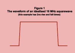
Figure 1 shows part of the waveform of an ideal 16 MHz square wave with 2 ns rise and fall times. This is what you would hope to see on your oscilloscope, although few people ever see anything that looks as good as this sketch!
Figure 2 shows its corresponding (idealised) frequency spectrum, which consists of a large number of narrow spectral lines at odd-numbered harmonics of the clock rate.

This is what you might see on a spectrum analyser or Fourier analyser when observing the signal in Figure 1. This sketch has a bold line drawn on it to show the envelope of the signal harmonics, and of course this line would not be drawn by a test instrument. Notice that the slope of the envelope is 20 dB/decade (identical to the schoolboy mnemonic: a third of the third, a fifth of the fifth, a seventh of the seventh, etc.) up to a frequency at which the slope increases to 40 dB/decade.
The frequency at which the slope changes from 20 to 40 dB/decade is governed by the rise and fall times of the waveform. For an ideal waveform such as that in figure 1 it is possible to calculate the slope-change point as the reciprocal of (rise/fall time multiplied by p), or "one over p tr". The usual text-book guidance is that the signal integrity or EMC designer need not concern themselves with the frequency content of their signals above this break-point, but real life has some unwelcome surprises. Real digital waveforms are not trapezoidal, especially when created by saturating logic (such as typical TTL or CMOS). The Cherry Clough Consultants Emissions Demonstration Unit uses F-TTL with a data sheet specification of 2 ns rise and fall times, and so "one over p tr" would imply that we can ignore frequencies above 170 MHz, but the unit's peak radiated emissions are at 643 MHz and it still has significant levels of emissions at well over 1 GHz.
Carrying on with our idealistic waveforms and spectra, we consider the "antenna effect" of an ideal 200 mm long straight PCB track on a typical FR4 glass-fibre PCB (Figure 3). This track is assumed to be all on its own, with no ground plane or other tracks anywhere nearby, driven by a perfect 0W source at one end and terminated at the other end by perfect 3/4W load. The "antenna effect" is my way of describing the non-ideality of the PCB track as a waveguide - the degree to which it leaks the electromagnetic waves it is supposed to be guiding from source to load into its surrounding environment (rather like a bucket with a hole in it leaks water to its environment instead of carrying it all the way to its destination).
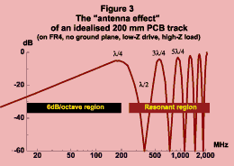
Figure 3 shows that starting from a low frequency, the track leaks progressively more as frequency increases, reaching its first peak at the frequency at which the electrical length of the track is one-quarter of the wavelength of a component of the signal (l/4). The wavelength (l) of a signal component is intimately related to its frequency (f) by the velocity (v) with which the wave propagates along the conductor: v = f l. The "electrical length" of a conductor depends upon the velocity of propagation of electromagnetic waves in it, and for FR4 the v is approximately half of what it is in free air. Consequently a track on FR4 reaches its first peak at half the frequency of the same length of wire surrounded by air. A length of track on FR4 has double the electrical length of the same physical length of wire in free air.
Electrical length is well known to designers trying to minimise the skew between signals and clocks in high-speed designs. In free air the velocity of propagation is approximately 1 ns per foot, or 3.3 ps per millimetre. On FR4 this slows to 2 ns per foot, or 6.6 ps per millimetre, which can make it very difficult to equalise trace lengths. On the ceramic substrates used in hybrid circuits and some military PCBs, the velocity of propagation is even lower. The material the copper wire or track is embedded in makes a difference to the velocity of propagation of the signal because the signal "really" travels as an electromagnetic wave in the surrounding medium - it has nothing to do with the speed of the electrons inside the conductor. The electromagnetic wave is the entire actual signal, and not just a side effect.
As we increase the frequency, figure 3 shows us that once past the first peak, the antenna effect of our ideal 200 mm PCB track goes into a trough which is deepest at exactly half the wavelength (l/2), from which it climbs out to a new peak at 3l/4, then to a trough at l, another peak at 5l/4, and so on to infinity. Our example ideal track behaves just the same way as an ideal whip antenna of twice its length (i.e. 400 mm).
It may be hard to see in this example why there are any signal currents, and consequently why it is that the physical structure of the return current path is important for signal integrity (which is a subset of EMC). To analyse this issue circuit designers (such as myself) generally ignore electromagnetic waves and think instead about what the conductor looks like terms of its intrinsic resistance, inductance, and capacitance. So that we can claim that the electromagnetic waves don't affect this analysis we consider the conductor to be made of lots of very short conductors all joined end-to-end, with each segment so short that it is very much shorter than the wavelengths concerned (at most: 1/100). The intrinsic space-charge capacitance of our thin PCB track is around 0.18 pF per millimetre, and current must flow into and out of this capacitance as signal voltage changes. This current must flow along the PCB track (maximum at the source, getting less towards the load end) and so must flow through the track's intrinsic inductance (approximately 1 nH per millimetre) and resistance. Resistance may be ignored at low frequencies, but increases due to skin effect at higher frequencies to the point where it can have significant effect - this is not considered in this article.
The changes of the signal's voltage applied to the track's capacitance gives rise to electric fields in the FR4 and air around the conductor, and the capacitor charging current flowing in the track inductance gives rise to magnetic fields around the conductor. So we always have currents flowing in any real conductor, even if it is terminated in a perfect 3/4W load, and the correct control of the EMC of the conductor, and the integrity of its signals, hinges upon controlling the return path of these currents. This analysis, which will be very familiar to designers who have wrestled with transmission lines has also given us a clue as to how it is that signals are "really" electric and magnetic fields which travel through the medium around their conductors.
Now let's see what happens when we connect the spectrum of our ideal signal waveform to our ideal 200 mm long PCB track with its antenna effects. Figure 4 shows that at the load end of the track we lose some of the signal's spectral content.

Notice that each peak and trough in figure 3 results in a dip in the harmonic envelope in figure 4. At frequencies at which figure 3 has a peak , figure 4 has a dip because a significant proportion of the signal at those frequencies has leaked away into the environment along the way. The frequencies at which figure 3 has a trough also gives us a dip in figure 4 because at these frequencies the track tends to looks like a short-circuit to the driver, and it finds it difficult to actually drive the track at all. (I know that a perfect driver should source infinite amounts of current into a short-circuit, so maybe I should not have shown such large dips at these frequencies, but in real life real drivers experience just this problem and the load suffers shortfalls in the frequency spectrum at both the peaks and troughs of the conductors' "antenna effects".)
Figure 5 shows the spectrum of the radiated emissions from the ideal 200 mm PCB track, and these have peaks where figure 3 has peaks, but they do not peak where figure 3 has troughs.
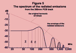
Notice that even with our ideal waveform, figure 5 shows radiated emissions at 1 GHz and over, and in real life the amplitude of these may be expected to be higher because the driver waveforms are generally not ideal trapezoids and have a higher high-frequency content. Products using clocks running above 100 MHz have clock waveforms with sub-nanosecond rise and fall times, and emission problems may be expected up to 5 GHz. When we start using 1 GHz clocks in real products we can expect emissions problems at even higher frequencies (and asynchronous logic will look like a very attractive alternative, for a number of reasons).
To complete the picture, Figure 6 shows the resulting waveforms at the load. The signal at the load shows a slowed rate of rise and fall, and significant overshoots and undershoots. The slow edges worsen the skew and the over/undershoots can cause false triggering when they exceed the noise margins. As an exercise for the mathematically-minded: try doing an inverse Fourier transform on the load spectrum of figure 4, it should come out looking just like the load waveform in figure 6.

EMC engineers tend to use spectrum analysers, so they may not be familiar with the other waveform shown on figure 6: the waveform of the radiated emissions. This contains much of the high frequency content that has been lost from the load signal.
This final waveform sketch leads us to realise that most of the time, when we measure a signal with an oscilloscope and find that it has degraded (slower edges, ringing, etc.), what we are actually learning is that we have radiated emissions which could cause a problem for EMC compliance, and could also cause a problem for crosstalk: the antennas of one conductor emitting and being picked up by the antennas of a different conductor. The upshot of this is that if we always measure load waveforms which are identical to the source waveforms, and if they show databook spec rise and fall times with a low amount of ringing, this is a powerful indicator that signal integrity is very good and EMC compliance is going to be very easy . Whenever our 'scopes reveal degraded waveforms they are really telling us that we have radiated emissions! An experienced EMC engineer can predict the radiated emissions and immunity performance of digital circuits from such 'scope pictures.
The waveforms of figure 6 are typical of the sort of thing we might see with a typical 250 MHz 'scope and probes fitted with flexible earth leads. With a very high frequency 'scope and probes, and good high-frequency probing techniques (no flexible probe earth leads) these waveforms look more like a series of rectangles rather than a decaying sine wave. From a typical digital transmission-line point of view these boxes reveal the reflections of the signal's edges at points in the transmission line where its characteristic impedance alters suddenly, such at an incorrectly terminated load. Dealing with signal integrity from a reflection standpoint is perfectly correct and effective, but does not reveal what the relationship with EMC is.
I realise that this article leaves out a lot of detailed, real-life issues, but its purpose was to show that EMC and signal integrity are really one and the same. Realising this shows how it is that EMC design from the beginning of a new design project has the ability to reduce time-to-market and unit manufacturing costs. Correct EMC design at signal-integrity level is a competitive tool that modern electronics manufacturers all need to employ to the full.
Proven good design practices for EMC at the signal integrity level do exist, and the main ones are described in my article "Fundamentals of Design for EMC" in the 1998 EMC & LVD Yearbook from Nutwood UK: phone 01208 851530, fax 01208 850871, e-mail nutwooduk@msn.com.
phone 01457 871 605, fax 01457 820 145, e-mail keith.armstrong@cherryclough.com
Archive Index
EMC Journal Home

© Nutwood UK Ltd 2001
|
Eddystone Court - De Lank Lane
St Breward - BODMIN - PL30 4NQ
Tel: +44 (0)1208 851530 - Fax: +44 (0)1208 850871
nutwooduk@nutwood.eu.com
|
|